FPGA Chip Structure
The current mainstream FPGA is still based on look-up table technology, which has far exceeded the basic performance of previous versions, and integrates hard-core (ASIC-type) modules for common functions such as RAM, clock management, and DSP. As shown in Figure 1-1 (Note: Figure 1-1 is just a schematic diagram, in fact, each series of FPGAs has its corresponding internal structure), the FPGA chip is mainly completed by 6 parts, namely: programmable input and output unit , basic programmable logic unit, complete clock management, embedded block RAM, rich wiring resources, embedded low-level functional units and embedded dedicated hardware modules

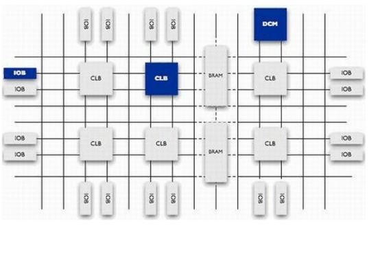
1. Programmable Input Output Unit (IOB)
The programmable input/output unit is referred to as the I/O unit, which is the interface part between the chip and the external circuit, and fulfills the driving and matching requirements for input/output signals under different electrical characteristics. Its schematic structure is shown in Figure 1-2. The I/O within the FPGA is categorized into groups, each of which can independently support a different I/O standard. Through the flexible configuration of the software, it can adapt to different electrical standards and I/O physical characteristics, adjust the drive current, and change the pull-up and pull-down resistors. At present, the frequency of I/O ports is also getting higher and higher, and some high-end FPGAs can support data rates up to 2Gbps through DDR register technology
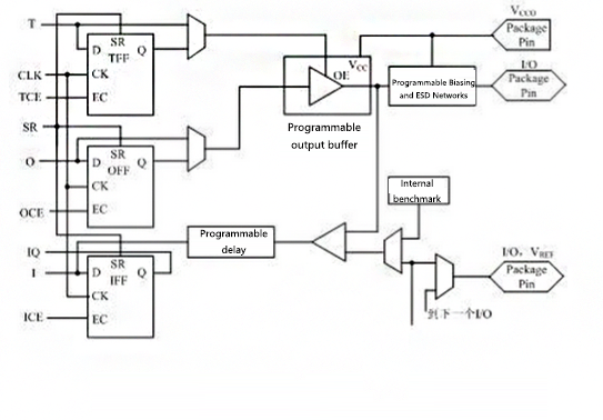
The external input signal can be input into the interior of the FPGA through the storage unit of the IOB module, or directly into the interior of the FPGA. When the external input signal is input into the FPGA through the storage unit of the IOB module, the requirement of its hold time (Hold TIme) can be reduced, which is usually 0 by default. In order to facilitate management and adapt to various electrical standards, the IOB of FPGA is divided into several groups (banks). The interface standard of each bank is determined by its interface voltage VCCO. A bank can only have one VCCO, but the VCCOs of different banks can different. Only ports of the same electrical standard can be connected together, the same VCCO voltage is the basic condition of the interface standard
2. Configurable Logic Block (CLB)
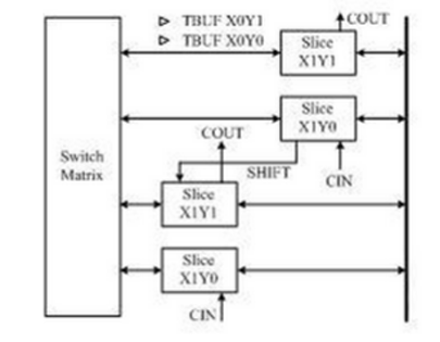
A CLB is the basic logic unit within an FPGA. The actual number and characteristics of CLBs will vary from device to device, but each CLB contains a configurable switch matrix consisting of 4 or 6 inputs, some selection circuitry (multiplexers, etc.), and flip-flops composition. The switch matrix is highly flexible and can be configured to handle combinational logic, shift registers or RAM. In Xilinx’s FPGA devices, the CLB consists of multiple (usually 4 or 2) identical slices and additional logic, as shown in Figure 1-3. Each CLB module can not only be used to implement combinational logic and sequential logic, but also can be configured as distributed RAM and distributed ROM.
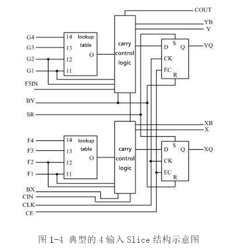
Slice is a basic logic unit defined by Xilinx, and its internal structure is shown in Figure 1-4. A slice consists of two 4-input functions, carry logic, arithmetic logic, storage logic and function multiplexer. Arithmetic logic includes an XOR gate (XORG) and a dedicated AND gate (MULTAND), an XOR gate can make a slice realize 2bit full addition operation, and the dedicated AND gate is used to improve the efficiency of the multiplier; the carry logic is determined by the dedicated carry signal. It is composed of a function multiplexer (MUXC) to implement fast arithmetic addition and subtraction operations; a 4-input function generator is used to implement a 4-input LUT, distributed RAM or a 16-bit shift register (in Slice of the Virtex-5 series chip). The two input functions are 6-input, which can realize 6-input LUT or 64-bit shift register); the carry logic includes two fast carry chains to improve the processing speed of the CLB module.
3. Digital Clock Management Module (DCM)
Most FPGAs in the industry offer digital clock management (all Xilinx FPGAs have this feature). Xilinx offers state-of-the-art FPGAs offering digital clock management and phase loop locking. Phase loop locking provides accurate clock synthesis with reduced jitter and filtering.
4. Embedded Block RAM (BRAM)
Most FPGAs have built-in block RAM, which greatly expands the application range and flexibility of FPGAs. Block RAM can be configured as single-port RAM, dual-port RAM, content-address memory (CAM), and common storage structures such as FIFO. RAM and FIFO are relatively popular concepts and will not be described here.
The CAM memory has a comparison logic in each of its internal storage units, the data written in the CAM will be compared with each internal data, and return the address of all data that is the same as the port data, so the address of the route is Switches have a wide range of applications. In addition to block RAM, LUTs in the FPGA can also be flexibly configured into structures such as RAM, ROM, and FIFO. In practical applications, the number of block RAMs inside the chip is also an important factor in choosing a chip.
For example: the capacity of a single-chip block RAM is 18k bits, that is, the bit width is 18 bits and the depth is 1024. The bit width and depth can be changed as needed, but two principles must be met: first, the modified capacity (bit width and depth) It cannot be larger than 18k bits; secondly, the maximum bit width cannot exceed 36 bits. Of course, multiple pieces of block RAM can be cascaded together to form a larger RAM, at this time, it is only limited by the number of block RAMs in the chip, and is no longer bound by the above two principles.
5. Rich wiring resources
The routing resources connect all the units inside the FPGA, and the length and process of the connection determine the driving ability and transmission speed of the signal on the connection. There are abundant wiring resources inside the FPGA chip, which are divided into 4 different categories according to the process, length, width and distribution position.
The first type is the global wiring resource, which is used for the wiring of the global clock and global reset/set within the chip; the second type is the long-line resource, which is used to complete the wiring of the high-speed signal between the chip banks and the second global clock signal; the third The first category is short-circuit resources, which are used to complete the logical interconnection and wiring between basic logic units; the fourth category is distributed routing resources, which are used for control signal lines such as exclusive clocks and resets.
In practice, the designer does not need to directly select routing resources, the placer can automatically select routing resources to connect each module unit according to the topology and constraints of the input logic netlist. Essentially, there is a close and direct relationship between the use of routing resources and the results of the design.
6. Bottom embedded functional unit
Embedded functional modules mainly refer to soft cores such as DLL (Delay Locked Loop), PLL (Phase Locked Loop), DSP and CPU. Nowadays, more and more embedded functional units have made a single-chip FPGA a system-level design tool, enabling it to have the ability to jointly design software and hardware, and gradually transition to a SOC platform.
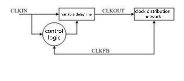
DLL and PLL have similar functions, and can complete the multiplication and division of clocks with high precision and low jitter, as well as duty cycle adjustment and phase shift functions. The chip produced by Xilinx Company integrates DLL, the chip of Altera Company integrates PLL, and the new chip of LatTIce Company integrates PLL and DLL at the same time. PLLs and DLLs can be easily managed and configured through IP core-generated tools. The structure of the DLL is shown in Figure 1-5
7. Embedded dedicated hard core
The embedded dedicated hard core is relative to the underlying embedded soft core, which refers to the hard core (Hard Core) with powerful FPGA processing capabilities, which is equivalent to an ASIC circuit. To improve FPGA performance, chip manufacturers integrate some dedicated hard cores inside the chip. For example, in order to improve the multiplication speed of FPGA, dedicated multipliers are integrated in mainstream FPGAs; in order to adapt to communication bus and interface standards, many high-end FPGAs have integrated serial-parallel transceivers (SERDES), which can reach tens of Gbps. Send and receive speed.
Xilinx’s high-end products not only integrate Power PC series CPUs, but also embed DSP Core modules. The corresponding system-level design tools are EDK and Platform Studio, and the concept of System on Chip is proposed accordingly. Through PowerPC, Miroblaze, Picoblaze and other platforms, standard DSP processors and related applications can be developed to achieve the development purpose of SOC.
7.1 soft core
In the field of EDA design, soft core refers to the register transfer level (RTL) model before synthesis; in FPGA design, it refers to the hardware language description of the circuit, including logic description, netlist and help documents. The soft core is only functionally simulated and needs to be synthesized and placed and routed before it can be used. Its advantages are high flexibility, strong portability, allowing users to self-configure; the disadvantage is that the predictability of the module is low, and there is a possibility of errors in subsequent design, and there are certain design risks. Soft cores are the most widely used form of IP cores.
7.2 solid core
In the field of EDA design, solid core refers to a netlist with floorplanning information; specifically, in FPGA design, it can be regarded as a softcore with floorplanning, which is usually provided in a mixed form of RTL code and corresponding specific process netlist. The RTL description is combined with the specific standard cell library for comprehensive optimization design to form a gate-level netlist, which can be used through the layout and routing tools. Compared with the soft core, the design flexibility of the solid core is slightly less, but the reliability is greatly improved. At present, solid core is also one of the mainstream forms of IP core.
7.3 hard core
In the field of EDA design, the hard core refers to the verified design layout; specifically, in the FPGA design, it refers to the design with fixed layout and process, verified by the front-end and back-end, and the designer cannot modify it. There are two reasons why it cannot be modified: first, the system design has strict timing requirements for each module, and it is not allowed to disrupt the existing physical layout; the second is the requirement to protect intellectual property rights, and designers are not allowed to make any changes to it. The non-modification feature of the IP hard core makes it difficult to reuse it, so it can only be used in some specific applications, and the scope of use is narrow.
Haoxinshengic is a pprofessional FPGA and IC chip supplier in China. We have more than 15 years in this field。 If you need chips or other electronic components and other products, please contact us in time. We have an ultra-high cost performance spot chip supply and look forward to cooperating with you.
If you want to know more about FPGA or want to purchase related chip products, please contact our senior technical experts, we will answer relevant questions for you as soon as possible
Our Products
